Room-size laser wakefield accelerators are going commercial. Here’s what that means for AI hardware, robotics automation, and resilient energy infrastructure.
Room-Size Particle Accelerators: A Practical Win
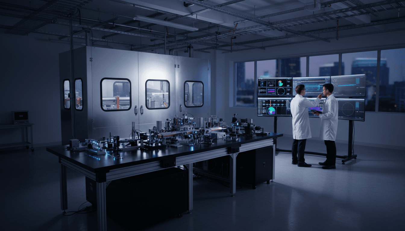
Particle accelerators have always had an image problem: they’re seen as cathedral-scale science projects—multi‑kilometer machines, national labs, and waiting lists. That assumption is starting to break.
A commercial laser wakefield accelerator—a room-size particle accelerator that uses an ultrashort, high-power laser to accelerate electrons—has now produced an electron beam in a productized system. The company behind it, TAU Systems, says customer access begins in 2026 via its Carlsbad, California facility. The headline isn’t “we hit a record energy.” It’s “we can do this reliably, repeatedly, and sell it.”
For anyone building AI-driven robotics, automation, and the energy infrastructure that supports them, this matters. Compute-heavy AI pushes demand for advanced chips, advanced chips pressure manufacturing and inspection, and that whole stack sits on power systems that have to be more resilient than ever. Compact accelerators touch that chain in three very practical places: radiation testing, high-speed imaging/inspection, and cheaper clinical-grade beams.
What a laser wakefield accelerator actually changes
A laser wakefield accelerator changes the economics and access of electron beams by collapsing a facility-scale capability into a room-scale tool.
Traditional accelerators get high energies by pushing particles through long radio-frequency structures. Wakefield accelerators do it differently: an intense ultrashort laser pulse hits a gas and creates a plasma. The plasma forms a wave (a “wake”), and electrons “surf” that wake to relativistic speeds. The fields can be extremely strong—often summarized as up to 1,000× higher accelerating gradients than conventional approaches—so the machine can be far shorter.
Here’s the commercially relevant part from the RSS summary: TAU’s first system targets 60–100 MeV electron beams at 100 Hz, with a stated upgrade path. They’re explicitly prioritizing stability and reproducibility over energy records, using a laser supplied by Thales.
“Reliability and reproducibility rather than record performance” is exactly the sentence you want to hear if you’re a buyer, not a physicist.
Why “commercial” matters more than “compact”
Labs have demonstrated wakefield acceleration for decades. Industry mostly couldn’t use it because day-to-day operation is brutally unforgiving:
- Beam stability affects test validity and imaging quality
- Laser uptime dictates throughput and scheduling
- Repeatability determines whether results stand up to audits and standards
A room-size accelerator that’s temperamental is a science exhibit. A room-size accelerator that’s boring to run becomes infrastructure.
The first real use case: radiation testing for space—and why utilities should care
The near-term application TAU highlights is radiation testing of electronics destined for satellites and spacecraft. Their claim is a 5–10× supply-demand gap for the most demanding tests.
That might sound niche if you work in energy and utilities, but the overlap is bigger than it looks:
Space-grade testing is a proxy for grid-grade resilience
Modern utilities are deploying more electronics in harsh environments and tighter footprints:
- Substation automation and protection relays
- Edge AI for fault detection and predictive maintenance
- Sensors on distributed energy resources (DERs)
- Communications hardware supporting grid orchestration
Space radiation is not the same as terrestrial stressors, but the engineering mindset is identical: understand failure modes early, qualify components faster, and avoid field failures that cascade.
If compact accelerators increase access to high-quality radiation tests, they can indirectly raise the baseline for “mission critical” electronics beyond aerospace—especially as climate-driven extremes push utilities toward tougher qualification regimes.
Why this is also an AI-in-robotics story
In this topic series (“AI in Robotics & Automation”), we often talk about smarter robots and automated plants. The unglamorous constraint is: robots are computers with actuators, and those computers are getting denser, hotter, and more sensitive.
More reliable radiation and stress testing improves:
- Robotics deployed in high-radiation settings (nuclear decommissioning, medical isotope production, space operations)
- Automation systems in energy facilities where downtime costs are measured in megawatt-hours
- Safety cases for autonomous inspection robots used in critical infrastructure
100–300 MeV: where imaging and chip inspection gets interesting
In the 100–300 MeV range, compact electron beams become credible drivers for high-precision, high-throughput imaging—including inspection of advanced 3D microchips.
That’s the bridge to AI, and it’s not abstract. AI performance trends keep pushing toward:
- Chiplet-based designs
- 3D stacking
- High-bandwidth memory integration
- More aggressive packaging
Those advances raise failure-analysis complexity. If you can’t “see” defects fast, you don’t just ship fewer chips—you slow the entire AI hardware cycle.
The bottleneck: inspection throughput, not just fabrication
Fabrication headlines get attention, but high-volume manufacturing lives and dies by metrology and failure analysis. TAU’s CEO claims current high-resolution failure analysis can take hours, while brighter next-generation sources could bring that to minutes or less.
Even if you discount the exact timing, the direction is right: more source brightness and more accessible beam time reduces the “debug loop” in manufacturing.
Here’s why energy and utilities should care: AI for grid optimization is compute-hungry. Better chips and faster manufacturing iteration reduce the cost of deploying models at scale—everything from transformer health analytics to real-time DER dispatch.
Practical examples of where faster chip imaging hits the real world
- Power electronics: SiC and GaN devices are increasingly common in inverters, fast chargers, and HVDC systems. Faster internal inspection means faster qualification and fewer nasty surprises.
- Edge AI modules: The more utilities push inference to the edge, the more they rely on advanced packaging in constrained thermal environments.
- Robotics controllers: Industrial robots used in energy asset maintenance depend on reliable high-density compute in harsh conditions.
300–1,000 MeV and the “manufacturing flywheel” for AI hardware
Higher energies (300–1,000 MeV) open the door to driving an X-ray free-electron laser (XFEL)—often described as among the brightest terrestrial X-ray sources.
This is where the story shifts from “a new tool for testing” to “a new tool for production economics.” TAU points to the possibility of next-generation X-ray lithography approaches that could push scaling further without rebuilding the whole fab concept.
You don’t need to bet on a specific lithography pathway to see the macro effect: if accelerators become smaller and cheaper, then more organizations can prototype, test, and iterate on manufacturing-adjacent ideas without waiting for scarce national facilities.
That matters because the AI/semiconductor/energy triangle is tightening:
- AI growth drives chip demand and power demand
- Chip manufacturing drives capital intensity and supply chain risk
- Power constraints increasingly shape where compute can be deployed
Reducing the friction in any leg of that triangle is economically meaningful.
What “$10M and up” means for real buyers
TAU’s stated pricing starts around US $10 million, with much of the cost in the ultrahigh-intensity laser.
For many teams, that price doesn’t scream “democratization.” For others, it’s a bargain compared with alternatives:
- Building or expanding a conventional accelerator facility
- Buying beam time at oversubscribed national labs
- Losing months in a product cycle waiting for qualification slots
A more realistic view: “democratization” means new access models
I don’t think most customers will buy one on day one. The more likely adoption pattern looks like this:
- Service model first: pay-per-use access at a vendor “showroom” facility (TAU is explicitly planning this)
- Dedicated installations: for aerospace primes, major chip players, and government labs
- Downmarket over time: as lasers mature into smaller, cheaper, more maintainable systems
If you’re in energy and utilities, the service model is the key: it creates a path to advanced qualification and imaging without capex shock.
How to evaluate a compact accelerator for industrial work
If your team is considering radiation testing or high-energy imaging services (or you’re just trying to plan partnerships), evaluate compact accelerators like you’d evaluate any automation platform: by throughput, repeatability, and integration.
The questions that separate demos from deployable tools
-
Beam stability and repeatability
- What’s the shot-to-shot energy spread and pointing stability?
- How often does it require recalibration?
-
Throughput and uptime
- 100 Hz sounds great; what’s sustained operation over an 8-hour day?
- What are typical maintenance intervals for the laser and target systems?
-
Dosimetry and traceability (for testing use cases)
- Can you produce audit-ready test reports?
- How is dose measured, logged, and verified?
-
Facility integration and safety
- Shielding requirements, interlocks, and operational staffing
- HVAC, power, and vibration sensitivity
-
Data pipeline (the AI tie-in most people miss)
- Imaging is only half the job; the other half is turning raw data into decisions.
- Ask what formats, APIs, and processing workflows are supported for automated analysis.
That last point is where this intersects strongly with AI in robotics & automation: once imaging and test data arrive faster, your bottleneck becomes analysis and decision automation—exactly what modern ML pipelines and industrial AI are good at.
Where this goes next for AI, robotics, and energy infrastructure
Room-size particle accelerators won’t replace national labs. They don’t need to. Their value is in taking a handful of high-impact workflows—radiation qualification, advanced imaging, faster failure analysis—and pulling them closer to everyday engineering.
For AI-driven automation, that means shorter iteration loops: better chips, quicker validation, faster deployment. For energy and utilities, it means a clearer path to resilient electronics and faster innovation in power hardware that has to survive decades in the field.
If 2026 is when commercial access begins, 2026–2028 is when we’ll find out who treats compact accelerators as a curiosity—and who treats them as a supply chain advantage.
The forward-looking question I’m watching: when accelerators become “room equipment” instead of “national infrastructure,” what other parts of the AI hardware pipeline get dragged into faster, more automated cycles?